Introduction
Jen-Hsun “Jensen” Huang stands as one of the most consequential and visionary figures in the history of modern computing and artificial intelligence. As the co-founder, president, and chief executive officer of NVIDIA Corporation, Huang has shepherded a relatively obscure graphics chip manufacturer into the foundational infrastructure provider of the twenty-first century’s artificial intelligence revolution. Over the course of more than three decades, his unwavering commitment to accelerated computing has fundamentally altered the trajectory of the technology industry, reshaping not only how video games are rendered, but how scientific research, enterprise computing, autonomous robotics, and generative artificial intelligence are executed on a global scale.
By 2026, Huang’s influence on the global economy and technological landscape reached unprecedented heights. Under his leadership, NVIDIA achieved a historic milestone by becoming the first company to surpass a $5 trillion market capitalization in October 2025, firmly establishing itself as the most valuable public enterprise in the world. This explosive growth was driven by an insatiable global demand for the computational power required to train and deploy advanced artificial intelligence models. As the architect of this silicon empire, Huang’s personal net worth eclipsed $200 billion, making him one of the wealthiest self-made individuals on the planet. Yet, despite his immense wealth and corporate power, Huang remains deeply involved in the intricate engineering and strategic product roadmaps of his company, famously operating without a traditional executive office and maintaining a flat organizational structure that allows him to interact directly with engineers and product managers.
Huang’s foresight to transition NVIDIA from a pure-play gaming hardware company into a general-purpose parallel computing juggernaut is widely regarded as one of the greatest strategic pivots in corporate history. By championing the Compute Unified Device Architecture (CUDA) and foreseeing the utility of graphics processing units (GPUs) for complex mathematical matrix operations, Huang laid the silicon groundwork for the deep learning boom. His leadership has been recognized universally, culminating in numerous global accolades, including the 2026 IEEE Medal of Honor, the 2025 Edison Achievement Award, and being recognized among the “Architects of AI” for TIME’s Person of the Year. This comprehensive biography details the life, technical innovations, leadership philosophy, and unparalleled achievements of Jensen Huang, tracing his journey from a young immigrant in rural America to the undisputed king of the artificial intelligence era.
Early Life and Heritage
Jensen Huang was born Jen-Hsun Huang on February 17, 1963, in the coastal city of Tainan, Taiwan. Born into a middle-class family, his early years were shaped by a rapidly changing geopolitical landscape in East Asia. His father worked as a chemical engineer, and his mother was a schoolteacher. When Huang was still a young child, his family relocated to Thailand, seeking new professional opportunities. However, the late 1960s and early 1970s were a period of intense volatility in Southeast Asia, largely due to the escalating conflict in neighboring Vietnam and widespread civil unrest in Thailand. Concerned for the safety and future of their children, Huang’s parents made the difficult decision to send Jensen and his older brother to the United States to live with relatives.
Upon arriving in the United States at the age of nine, Huang’s life took an unexpected turn. His aunt and uncle, who were recent immigrants themselves and largely unfamiliar with the American educational system, mistakenly enrolled Jensen and his brother in the Oneida Baptist Institute in rural Kentucky. Believing it to be a prestigious preparatory academy, they were unaware that the institution was actually a religious reform school designed primarily for troubled youth. At Oneida, Huang was thrust into a rugged, unforgiving environment. He was one of the youngest students at the school and the only one of Asian descent. To earn his keep and contribute to the school’s maintenance, Huang was assigned the daily chore of cleaning the boys’ dormitories, including scrubbing the communal toilets. Rather than breaking his spirit, this grueling experience instilled in him a profound sense of resilience, discipline, and a formidable work ethic that would define his future entrepreneurial endeavors. Huang would later reflect on his time in Kentucky not with bitterness, but with gratitude for the mental toughness it cultivated.
After a couple of years in Kentucky, Huang’s parents were finally able to secure passage to the United States, reuniting the family and settling in the Pacific Northwest, specifically in the suburbs of Portland, Oregon. Here, Huang attended Aloha High School. In this more stable environment, he began to flourish both academically and athletically. He discovered a deep passion for competitive table tennis, dedicating countless hours to mastering the sport. His relentless practice paid off when he became a nationally ranked junior table tennis player. The intense focus, strategic thinking, and fast-paced reaction times required for competitive table tennis mirrored the cognitive skills he would later apply to the fast-moving semiconductor industry. During his high school years, Huang also demonstrated a natural aptitude for mathematics and science, subjects that provided a logical foundation for his burgeoning interest in the emerging world of electronics and computing.
Academic Journey
Following his graduation from Aloha High School, Huang chose to remain in the Pacific Northwest for his undergraduate studies, enrolling at Oregon State University (OSU) in Corvallis. He pursued a Bachelor of Science degree in Electrical Engineering, a field that was rapidly evolving as the microprocessor revolution began to take hold. At OSU, Huang immersed himself in the complexities of circuit design, computer architecture, and solid-state physics. It was also in the electrical engineering laboratories of OSU that Huang met his future wife, Lori Mills, who was his engineering lab partner. Their shared passion for technology and engineering formed the basis of a lifelong partnership.
Huang proved to be an exceptional student, absorbing the foundational principles of electrical engineering with ease. However, he also recognized that the true epicenter of the computing revolution was located further south, in the Santa Clara Valley of California—widely known as Silicon Valley. Upon earning his Bachelor of Science in Electrical Engineering (BSEE) in 1984, Huang and Lori relocated to the San Francisco Bay Area. Eager to deepen his technical expertise while simultaneously launching his professional career, Huang applied to the master’s program at Stanford University.
Stanford University offered an unparalleled academic environment, heavily intertwined with the booming venture capital ecosystem and the pioneering technology firms of Silicon Valley. Because he was working full-time in the semiconductor industry, Huang attended Stanford as a part-time student, taking evening and weekend classes. This grueling schedule required him to balance the demanding theoretical coursework of a premier graduate institution with the intense, deadline-driven pressures of his day jobs. The dual exposure to cutting-edge academic research and ruthless corporate engineering proved invaluable. At Stanford, Huang was exposed to advanced concepts in Very Large Scale Integration (VLSI) design and microprocessor architecture. He officially earned his Master of Science in Electrical Engineering (MSEE) from Stanford University in 1992, completing an educational foundation that bridged the gap between theoretical computer science and practical, commercial silicon fabrication.
Early Career in Silicon Valley
Jensen Huang’s professional career began in 1984 at Advanced Micro Devices (AMD), a company that would eventually become one of NVIDIA’s fiercest competitors. At AMD, Huang worked as a microprocessor designer. This role provided him with firsthand experience in the intricate process of laying out logic gates, optimizing instruction sets, and understanding the physical limitations of silicon wafers. Although his tenure at AMD was relatively brief, lasting only a little over a year, it was a critical apprenticeship that taught him the fundamental mechanics of the semiconductor business.
In 1985, Huang transitioned to LSI Logic, a pioneering company in the field of Application-Specific Integrated Circuits (ASICs). Over the next eight years, Huang rose through the ranks at LSI Logic, transitioning from a pure engineering role into engineering management and eventually product strategy. He became the Director of the Coreware division, a role that required a deep understanding of both technological capabilities and market demands. LSI Logic was at the forefront of the “System-on-a-Chip” (SoC) methodology, allowing customers to design custom silicon by combining pre-designed intellectual property (IP) blocks with custom logic. This role taught Huang a crucial business lesson: the value of building flexible, scalable architectures that could address a wide variety of customer needs.
More importantly, his time at LSI Logic exposed Huang to the “fabless” semiconductor business model. Historically, semiconductor companies like Intel and IBM owned their own fabrication plants (fabs), a massive capital expenditure that required billions of dollars in upkeep and constant modernization. LSI Logic and others were proving that it was possible to decouple the design of the chip from the manufacturing of the chip, outsourcing the fabrication to specialized foundries in Asia. This realization—that a company could focus entirely on intellectual property, architecture, and software without bearing the crushing overhead of a silicon fab—would become the foundational economic premise upon which Huang would build NVIDIA.
The Founding of NVIDIA
The genesis of NVIDIA can be traced back to a fateful meeting in early 1993 at a Denny’s diner on Berryessa Road in San Jose, California. Huang, then 30 years old, sat down with two seasoned microchip engineers from Sun Microsystems: Chris Malachowsky and Curtis Priem. Over endless cups of coffee, the trio discussed the future of computing. At the time, the personal computer was primarily a text-based, utilitarian device used for word processing and spreadsheets. However, the three engineers shared a visionary thesis: the next major leap in computing would be driven by the demand for complex, real-time 3D graphics, primarily fueled by the burgeoning video game industry.
They recognized that the central processing unit (CPU), which executed tasks in a sequential manner, was fundamentally ill-equipped to handle the massive parallel calculations required to render millions of pixels and polygons on a screen 60 times a second. They envisioned a dedicated graphics co-processor—a concept that did not yet have a name—that would sit alongside the CPU and handle the intense mathematical workloads of 3D rendering. Convinced of this vision, Huang left his comfortable position at LSI Logic, and Malachowsky and Priem departed Sun Microsystems to start a new venture.
The founders initially had no name for their company, naming all their early files “NV” for “next version.” When they finally needed to incorporate, they looked for words containing those two letters. They discovered the Latin word “invidia,” meaning “envy,” and modified it slightly to create NVIDIA. Their goal was to build graphics chips so powerful that their competitors would be green with envy—a concept that later inspired the company’s iconic green eye logo.
To fund their ambitious vision, Huang approached Don Valentine, the legendary founder of Sequoia Capital. Valentine was notoriously tough, but he was impressed by Huang’s deep technical knowledge and unyielding conviction. Sequoia Capital, alongside Sutter Hill Ventures, provided the initial $20 million in venture funding to launch the company. True to the lessons Huang learned at LSI Logic, NVIDIA was founded as a strictly fabless semiconductor company. They would focus all their resources on architecture, drivers, and design, and rely on external foundries to manufacture the chips. To achieve this, Huang forged a critical early relationship with Morris Chang, the founder of Taiwan Semiconductor Manufacturing Company (TSMC). This partnership between NVIDIA and TSMC would not only secure NVIDIA’s supply chain but would eventually grow into one of the most important symbiotic business relationships in the global technology sector.
The Early Struggles and the NV1
Despite their grand vision and ample funding, NVIDIA’s first foray into the market was nearly its last. In 1995, the company released its first product, the NV1. It was an immensely ambitious, highly integrated multimedia chip. In an era before standardized graphics APIs (Application Programming Interfaces), the NV1 attempted to do everything: it processed 2D graphics, 3D graphics, audio, and even featured integrated Sega Saturn gamepad ports. However, the most controversial aspect of the NV1 was its architectural approach to 3D rendering. Instead of using triangles and polygons—the industry standard for creating 3D models—the NV1 utilized “quadratic texture mapping,” drawing surfaces using curved equations.
This architectural gamble proved disastrous. Shortly after the NV1’s release, Microsoft unveiled DirectX (specifically Direct3D), a standardized graphics API for Windows that explicitly required polygon-based rendering. Because the NV1 used quadrilaterals, it was fundamentally incompatible with the new Microsoft standard, making it exceedingly difficult for game developers to write software for the chip. The NV1 was a commercial failure, and NVIDIA found itself rapidly burning through its venture capital.
With the company facing imminent bankruptcy, its survival hinged on a contract with the Japanese gaming giant SEGA. SEGA had hired NVIDIA to design the graphics processor for their upcoming Dreamcast console, a project internally codenamed NV2. Like the NV1, the NV2 was based on quadratic rendering. Midway through the development cycle, Huang realized that quadratic rendering was a technological dead end and that the future belonged undeniably to polygons. He faced a severe moral and business dilemma: continue taking SEGA’s money to build a chip he knew would fail, or tell the truth and risk the immediate liquidation of his company.
Huang chose the latter. In a pivotal meeting with SEGA CEO Shoichiro Irimajiri, Huang confessed that the NV2 architecture was flawed, that NVIDIA could not deliver the chip SEGA needed, and that SEGA should look to another vendor. However, Huang also explained that NVIDIA would go bankrupt if SEGA simply canceled the contract, and he boldly asked Irimajiri to pay NVIDIA in full for the unfinished, canceled project. In an extraordinary act of corporate grace and belief in Huang’s integrity, Irimajiri convinced SEGA’s management to invest $5 million into NVIDIA, effectively buying out the contract. This lifeline provided NVIDIA with just enough capital to survive for a few more months and pivot their entire architecture toward polygons.
The Turning Point: RIVA 128 and the GeForce Era
Armed with SEGA’s crucial financial lifeline, Huang ruthlessly restructured NVIDIA. He laid off a significant portion of the staff and focused the remaining engineers on a singular, do-or-die project: the NV3, later known as the RIVA 128. Released in 1997, the RIVA 128 was a polygon-based 3D accelerator that fully supported Microsoft’s Direct3D. It was designed with one overriding objective: raw speed. The RIVA 128 was a massive commercial success, offering superior performance to its competitors at a competitive price. It saved NVIDIA from the brink of collapse and established the company as a formidable player in the graphics market.
Recognizing the brutal pace of the semiconductor industry, Huang instituted a punishing product development cycle. While competitors operated on an 18-to-24-month design cycle, Huang mandated that NVIDIA release a new, vastly improved architectural generation every six months. This aggressive cadence, often referred to internally as “Huang’s Law,” outpaced the legendary Moore’s Law and completely overwhelmed the competition. NVIDIA’s primary rival, 3dfx Interactive—creator of the famous Voodoo graphics cards—was unable to keep up with NVIDIA’s relentless execution. By late 2000, NVIDIA acquired the intellectual property and assets of a bankrupt 3dfx, securing total dominance in the PC graphics sector.
In January 1999, Huang took NVIDIA public on the NASDAQ exchange. Later that same year, NVIDIA released the GeForce 256. With this product, Huang and his marketing team coined a new term: the Graphics Processing Unit (GPU). The GeForce 256 was revolutionary because it integrated Hardware Transform and Lighting (T&L) directly onto the silicon. Previously, calculating the geometry of a 3D scene and its lighting was handled by the CPU. By offloading these massive parallel calculations to the GPU, NVIDIA freed up the CPU to handle game logic and artificial intelligence, fundamentally altering the architecture of the modern personal computer. This technological leap caught the attention of Microsoft, leading to NVIDIA securing the exclusive contract to supply the graphics hardware for the original Xbox console, cementing the company’s status as a Silicon Valley titan.
The CUDA Revolution: A Billion-Dollar Gamble
While dominating the gaming industry was highly profitable, Jensen Huang harbored a much grander vision for the GPU. He observed that the highly parallel architecture of the GPU—featuring thousands of tiny processing cores designed to render millions of pixels simultaneously—could theoretically be used to solve complex mathematical problems far faster than standard sequential CPUs. However, utilizing a graphics card for non-graphics mathematics was incredibly difficult; programmers had to trick the GPU by translating their mathematical equations into graphics rendering problems (a practice known as GPGPU, or General-Purpose computing on GPUs).
In 2006, Huang made the most consequential, and risky, decision of his career. Under his direction, NVIDIA announced CUDA (Compute Unified Device Architecture). CUDA was a revolutionary software platform and programming interface that allowed developers to write standard C/C++ code and execute it directly on the GPU’s parallel processing cores, completely bypassing the graphics pipeline. To make CUDA work, NVIDIA had to fundamentally redesign its hardware, adding specific logic to every single GPU they manufactured, from the cheapest laptop chip to the most expensive desktop card.
This decision came at a massive cost. The research, development, and silicon real estate required for CUDA cost NVIDIA billions of dollars. Furthermore, for years, there was virtually no commercial market for it. The gaming community didn’t care about scientific computing, and the scientific community was slow to adopt the new platform. NVIDIA’s profit margins collapsed, and the company’s stock price plummeted. Wall Street analysts and furious shareholders aggressively pressured Huang to abandon CUDA, arguing that it was a vanity project that was destroying shareholder value.
Huang, however, demonstrated unyielding conviction. He absorbed the intense criticism, protected his engineering teams, and refused to back down. He believed that if NVIDIA built the parallel computing platform, researchers in fields like molecular dynamics, quantum chemistry, fluid dynamics, and astrophysics would eventually realize its power. Slowly, his prediction came true. Supercomputing centers began clustering NVIDIA GPUs to achieve unprecedented floating-point performance, establishing NVIDIA’s foothold in the high-performance computing (HPC) market. But even Huang could not have predicted the specific application that would vindicate his billion-dollar gamble and change the world.
The AI Awakening: AlexNet and the Deep Learning Boom
The vindication of CUDA arrived in 2012 during the ImageNet Large Scale Visual Recognition Challenge, a global competition for computer vision algorithms. For years, progress in artificial intelligence had been stagnant, hampered by the inability of standard CPUs to process massive datasets quickly enough to train deep neural networks. A team of researchers from the University of Toronto—Geoffrey Hinton, Alex Krizhevsky, and Ilya Sutskever—decided to use a fundamentally different approach. They wrote their convolutional neural network, dubbed AlexNet, using NVIDIA’s CUDA platform and trained it on two consumer-grade NVIDIA GTX 580 graphics cards.
AlexNet destroyed the competition, recognizing images with an accuracy that shattered previous records. The researchers realized that the matrix multiplication required to train deep neural networks was mathematically identical to the operations GPUs used to render 3D graphics. A GPU could train in days a neural network that would take a CPU months to process.
When Huang saw the results of the ImageNet competition, he experienced a profound epiphany. He recognized that deep learning was not just a new software technique, but an entirely new paradigm of computing where software writes software. In a move of characteristic decisiveness, Huang ordered a massive strategic pivot. He directed nearly every engineering resource within NVIDIA to focus on artificial intelligence. The company began optimizing its silicon architectures specifically for neural networks and rapidly expanded its software libraries to support AI frameworks like TensorFlow and PyTorch.
In 2016, to signal NVIDIA’s total commitment to this new era, Huang hand-delivered the world’s first AI supercomputer in a box, the DGX-1, to a then-nascent non-profit research lab in San Francisco called OpenAI. The device was received by Elon Musk and Sam Altman. The DGX-1, packed with eight powerful GPUs and optimized exclusively for deep learning, dramatically accelerated OpenAI’s research capabilities, setting the stage for the generative AI revolution that was soon to follow.
Architectural Evolution: From Fermi to Hopper
Under Huang’s leadership, NVIDIA’s hardware roadmap became entirely focused on maximizing AI throughput, leading to a rapid succession of groundbreaking microarchitectures, each named after a famous scientist. The true modern era began with the Fermi architecture in 2010, which laid the rigorous groundwork for double-precision computing, followed by Kepler (2012), Maxwell (2014), and Pascal (2016), which introduced high-bandwidth memory (HBM) and NVLink, a high-speed interconnect that allowed multiple GPUs to pool their memory and act as a single massive accelerator.
The true inflection point for AI hardware occurred with the Volta architecture in 2017. Under Huang’s direction, the engineering team introduced a radical new hardware component: the Tensor Core. Unlike standard CUDA cores designed for general graphics math, Tensor Cores were highly specialized circuits designed to do one thing—massive matrix multiplication for deep learning—at unprecedented speeds. This dedicated hardware acceleration resulted in exponential performance gains for AI training and inference.
Volta was followed by the Turing architecture in 2018, which introduced hardware acceleration for real-time ray tracing, revolutionizing computer graphics yet again. But in the data center, the focus remained on AI. The Ampere architecture (2020), specifically the A100 GPU, became the universal engine of the AI cloud, bought in massive quantities by hyperscalers like Amazon Web Services, Google Cloud, and Microsoft Azure.
However, it was the Hopper architecture, announced in 2022 and featuring the H100 GPU, that would power a paradigm shift. Hopper introduced the Transformer Engine, specialized hardware specifically designed to accelerate Transformer models—the underlying architecture of Large Language Models (LLMs). The H100 offered an order-of-magnitude leap in performance over the A100, perfectly timed to meet the explosion in demand that was about to occur.
The Generative AI Era and Trillion-Dollar Milestones
In late 2022, OpenAI released ChatGPT, a generative AI application powered entirely by thousands of NVIDIA GPUs. ChatGPT’s ability to understand context, write code, and generate human-like text sent shockwaves through the global technology industry. An AI arms race immediately commenced among tech giants, startups, and sovereign nations, all desperate to train their own frontier models. The constraint was no longer data or algorithms; the absolute bottleneck was compute power, specifically the NVIDIA H100 GPU.
Demand for NVIDIA’s hardware skyrocketed to unprecedented levels. Companies placed orders for tens of thousands of GPUs, leading to massive supply shortages. Jensen Huang had successfully transformed NVIDIA from a chip vendor into the sole arms dealer of the AI revolution. Because NVIDIA controlled both the premier hardware (the H100) and the indispensable software ecosystem (CUDA, which developers had been using for 15 years), the company possessed an impenetrable competitive moat.
The financial results were staggering. Quarter after quarter throughout 2023 and 2024, NVIDIA shattered Wall Street’s revenue and profit expectations. In May 2023, NVIDIA’s market capitalization surpassed $1 trillion. Driven by the relentless deployment of AI infrastructure, the stock continued to surge. In early 2024, the company broke the $2 trillion mark, and shortly thereafter, the $3 trillion mark, briefly surpassing Apple and Microsoft. The momentum did not slow; as AI models became larger and required exponentially more compute, NVIDIA’s valuation soared past $4 trillion, and by October 2025, NVIDIA made history as the first enterprise to surpass a $5 trillion market capitalization. Jensen Huang had realized his vision of the “AI Factory”—massive data centers dedicated not to storing data, but to manufacturing intelligence.
The Next Generation: Blackwell and Vera Rubin
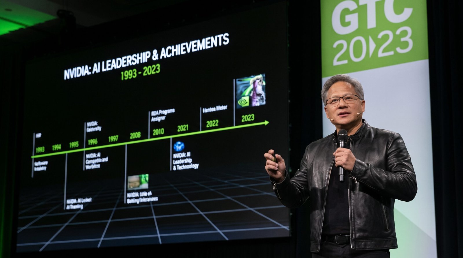
Refusing to rest on his laurels, Huang accelerated NVIDIA’s innovation engine. At the 2024 GPU Technology Conference (GTC), he unveiled the Blackwell architecture, named after mathematician David Blackwell. The flagship B200 GPU and the GB200 superchip (which tightly coupled the GPU with NVIDIA’s Grace CPU) offered massive leaps in parameter handling and energy efficiency for trillion-parameter LLMs. In 2025, the company released the highly anticipated Blackwell Ultra to meet the insatiable inference demands of deployed AI agents.
However, it was Huang’s GTC 2026 keynote that solidified NVIDIA’s dominance for the remainder of the decade. During this historic presentation, Huang unveiled the Vera Rubin architecture, the successor to Blackwell, named in honor of the pioneering astronomer who provided evidence of dark matter. Slated for full deployment in late 2026 and 2027, the Rubin architecture introduced a revolutionary combined GPU-HBM (CG-HBM) memory design, stacking memory directly on the compute die to eliminate the chronic memory bandwidth bottlenecks in LLM inference. The architecture was specifically optimized for Mixture-of-Experts (MoE) model designs, drastically improving the compute density and power efficiency per FLOP.
During the same 2026 keynote, Huang signaled NVIDIA’s aggressive expansion beyond raw silicon into software and physical systems. He introduced NemoClaw, an enterprise software platform for rapid model customization, and pushed heavily into “Physical AI,” releasing the Neotron 3 Super chip designed for edge AI inference in autonomous robotics and industrial automation. In an unprecedented move demonstrating total supply chain dominance, Huang provided a three-generation visibility roadmap, confirming the Vera Rubin architecture, its Ultra successor, and announcing the subsequent “Feynman” architecture slated for 2028. This relentless cadence ensured that hyperscalers attempting to transition to competing silicon would be consistently outpaced by NVIDIA’s execution.
Leadership Philosophy and Corporate Culture
Jensen Huang’s leadership style is as unique as the technology his company creates. Over three decades at the helm, he has cultivated a corporate culture designed explicitly for speed, agility, and the rapid assimilation of new information. Unlike traditional corporate structures that rely on strict hierarchies and deep layers of middle management, Huang operates NVIDIA as an extremely flat organization. As CEO, he directly manages over 50 direct reports. This wide span of control is intentional; it prevents information from being filtered, diluted, or delayed as it moves up the chain of command.
Huang famously abhors traditional corporate rituals. He does not hold regular one-on-one meetings with his executives, nor does he require formal status reports. Instead, he relies on a practice where employees, regardless of their rank, are encouraged to email him a brief list of the “top five things on their mind.” Huang reads these emails religiously, allowing him to keep a real-time pulse on the technical challenges and breakthroughs happening at the lowest levels of the engineering stack. He is known to drop into random meetings and interrogate engineers using first-principles thinking, demanding rigorous intellectual honesty.
Central to Huang’s philosophy is a deeply ingrained paranoia, a byproduct of NVIDIA’s near-death experiences in its early years. He frequently reminds his employees that “our company is 30 days from going out of business.” This mantra is not meant to paralyze the workforce with fear, but to foster an environment where complacency is eradicated, and urgency is the default state. Huang champions a high tolerance for failure, provided that the failure is the result of taking a calculated risk to solve a massively complex problem. He focuses NVIDIA on “zero-billion-dollar markets”—technological frontiers that do not yet exist, but which NVIDIA can create through sheer innovation.
Visually, Huang has cultivated an iconic personal brand, universally recognized for his uniform: black jeans, a black t-shirt, and his trademark black leather jacket. This consistent attire eliminates decision fatigue and mirrors his focused, unpretentious approach to business.
Philanthropy and Personal Life
Despite his status as a centibillionaire, Jensen Huang maintains a relatively private personal life. He and his wife, Lori Huang, whom he met in the electrical engineering labs at Oregon State University, have been married since 1985. They have two children, Spencer and Madison, both of whom have carved out successful careers outside the immediate shadow of their father’s tech empire. The Huangs maintain a residence in Los Altos, California, keeping them close to NVIDIA’s sprawling, futuristic headquarters in Santa Clara.
In his philanthropic endeavors, Huang has heavily prioritized the institutions that shaped his early life and career. Recognizing the pivotal role of academic research in technology, Huang has been a major benefactor to higher education. He and Lori donated $30 million to Stanford University to fund the Jen-Hsun Huang Engineering Center, a state-of-the-art facility designed to foster interdisciplinary engineering research.
Equally devoted to his undergraduate alma mater, Huang donated a staggering $50 million to Oregon State University in 2022 to establish a namesake collaborative innovation complex, featuring one of the nation’s most powerful university-based supercomputers. This donation aims to position OSU at the forefront of AI and robotics research. Furthermore, Huang has never forgotten the challenging years he spent at the Oneida Baptist Institute in Kentucky; he has quietly funded the construction of new academic buildings and dormitories at the school, ensuring that future generations of students have a more supportive environment than the one he encountered.
In a fascinating twist of Silicon Valley genealogy, Jensen Huang is closely related to another titan of the semiconductor industry: Dr. Lisa Su, the CEO of Advanced Micro Devices (AMD)—the very company where Huang began his career and NVIDIA’s primary competitor in the GPU space. Su is Huang’s first cousin once removed, adding a deeply personal layer of rivalry and shared brilliance to the global processor wars.
Awards and Global Recognition
Jensen Huang’s singular contribution to the advent of the AI era has resulted in an exhaustive list of global honors from engineering societies, business publications, and international organizations. Early in his career, he was named Entrepreneur of the Year in High Technology by Ernst & Young (1999) and received the Dr. Morris Chang Exemplary Leadership Award (2004). As NVIDIA’s dominance in accelerated computing became undeniable, the prestigious awards multiplied. He was awarded the Robert N. Noyce Award from the Semiconductor Industry Association in 2021, representing the semiconductor industry’s highest honor.
Time magazine has repeatedly recognized his global influence, including him in the Time 100 list in 2021 and 2024, and naming him among the “Architects of AI” for Time’s Person of the Year in 2025. In February 2024, Huang achieved one of the most significant academic honors an engineer can receive when he was elected to the National Academy of Engineering for his role in fueling the artificial intelligence revolution through high-powered GPUs. Late 2024 saw Huang awarded the prestigious Edison Achievement Award for his visionary leadership in AI, followed by receiving the grand prize of the VinFuture Prize alongside the foundational “Godfathers of AI” (Yoshua Bengio, Yann LeCun, and Geoffrey Hinton).
The pinnacle of his professional recognition arrived in 2026, when the Institute of Electrical and Electronics Engineers (IEEE)—the world’s largest technical professional organization—selected Huang as the recipient of the 2026 IEEE Medal of Honor. Accompanied by a $2 million prize, this award cited his pioneering leadership in accelerated computing and his transformative role in positioning NVIDIA at the forefront of technological innovation. As of 2026, holding honorary doctorates from National Taiwan University, Oregon State University, and Hong Kong University of Science and Technology, Jensen Huang stands not merely as a successful chief executive, but as the foundational architect of the artificial intelligence industrial revolution.